- 您现在的位置:买卖IC网 > Sheet目录3873 > PIC16CR76T-I/SS (Microchip Technology)IC PIC MCU 8KX14 28SSOP
2007 Microchip Technology Inc.
DS21993C-page 9
PIC16CR7X
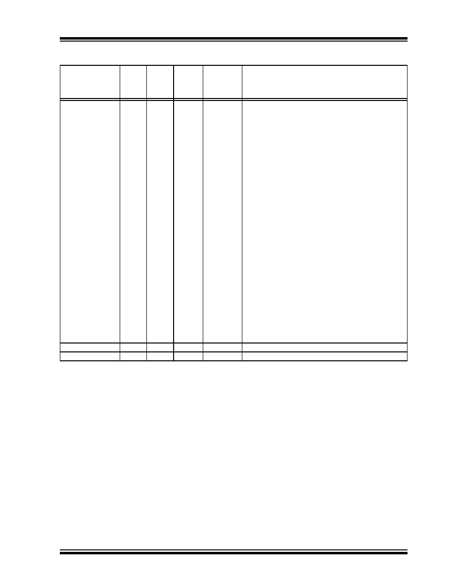
PORTC is a bidirectional I/O port.
RC0/T1OSO/T1CKI
RC0
T1OSO
T1CKI
11
8
I/O
O
I
ST
Digital I/O.
Timer1 oscillator output.
Timer1 external clock input.
RC1/T1OSI/CCP2
RC1
T1OSI
CCP2
12
9
I/O
I
I/O
ST
Digital I/O.
Timer1 oscillator input.
Capture2 input, Compare2 output, PWM2 output.
RC2/CCP1
RC2
CCP1
13
10
I/O
ST
Digital I/O.
Capture1 input/Compare1 output/PWM1 output.
RC3/SCK/SCL
RC3
SCK
SCL
14
11
I/O
ST
Digital I/O.
Synchronous serial clock input/output for SPI mode.
Synchronous serial clock input/output for I2C mode.
RC4/SDI/SDA
RC4
SDI
SDA
15
12
I/O
I
I/O
ST
Digital I/O.
SPI data in.
I2C data I/O.
RC5/SDO
RC5
SDO
16
13
I/O
O
ST
Digital I/O.
SPI data out.
RC6/TX/CK
RC6
TX
CK
17
14
I/O
O
I/O
ST
Digital I/O.
USART asynchronous transmit.
USART 1 synchronous clock.
RC7/RX/DT
RC7
RX
DT
18
15
I/O
I
I/O
ST
Digital I/O.
USART asynchronous receive.
USART synchronous data.
VSS
8, 19
5, 16
P
—
Ground reference for logic and I/O pins.
VDD
20
17
P
—
Positive supply for logic and I/O pins.
TABLE 1-2:
PIC16CR73 AND PIC16CR76 PINOUT DESCRIPTION (CONTINUED)
Pin Name
PDIP
SSOP
SOIC
Pin#
MLF
Pin#
I/O/P
Type
Buffer
Type
Description
Legend:
I = input
O = output
I/O = input/output
P = power
— = Not used
TTL = TTL input
ST = Schmitt Trigger input
Note
1:
This buffer is a Schmitt Trigger input when configured as the external interrupt.
2:
This buffer is a Schmitt Trigger input when used in Serial Verify mode.
3:
This buffer is a Schmitt Trigger input when configured in RC Oscillator mode and a CMOS input otherwise.
发布紧急采购,3分钟左右您将得到回复。
相关PDF资料
PIC18F13K50-I/P
IC PIC MCU FLASH 4KX16 20-PDIP
PIC16CR76T-I/SO
IC PIC MCU 8KX14 28SOIC
PIC18LF24K22-I/MV
IC PIC MCU 16KB FLASH 28UQFN
PIC18LF24K22-I/ML
IC PIC MCU 16KB FLASH 28QFN
PIC16CR76T-I/ML
IC PIC MCU 8KX14 28QFN
PIC16F627-04/P
IC MCU FLASH 1KX14 COMP 18DIP
PIC18F45J10-I/ML
IC PIC MCU FLASH 16KX16 44QFN
PIC18F24K22-I/ML
IC PIC MCU 16KB FLASH 28QFN
相关代理商/技术参数
PIC16CR77-I/ML
功能描述:IC PIC MCU 8KX14 44QFN RoHS:是 类别:集成电路 (IC) >> 嵌入式 - 微控制器, 系列:PIC® 16C 产品培训模块:Asynchronous Stimulus
8-bit PIC® Microcontroller Portfolio 标准包装:42 系列:PIC® 16C 核心处理器:PIC 芯体尺寸:8-位 速度:20MHz 连通性:- 外围设备:欠压检测/复位,POR,PWM,WDT 输入/输出数:13 程序存储器容量:3.5KB(2K x 14) 程序存储器类型:OTP EEPROM 大小:- RAM 容量:128 x 8 电压 - 电源 (Vcc/Vdd):4 V ~ 5.5 V 数据转换器:A/D 4x8b 振荡器型:外部 工作温度:-40°C ~ 85°C 封装/外壳:18-SOIC(0.295",7.50mm 宽) 包装:管件 配用:XLT18SO-1-ND - SOCKET TRANSITION 18SOIC 300MILISPICR1-ND - ADAPTER IN-CIRCUIT PROGRAMMING309-1011-ND - ADAPTER 18-SOIC TO 18-DIP309-1010-ND - ADAPTER 18-SOIC TO 18-DIPAC164010-ND - MODULE SKT PROMATEII DIP/SOIC
PIC16CR77-I/P
功能描述:IC PIC MCU 8KX14 40DIP RoHS:是 类别:集成电路 (IC) >> 嵌入式 - 微控制器, 系列:PIC® 16C 产品培训模块:Asynchronous Stimulus
8-bit PIC® Microcontroller Portfolio 标准包装:42 系列:PIC® 16C 核心处理器:PIC 芯体尺寸:8-位 速度:20MHz 连通性:- 外围设备:欠压检测/复位,POR,PWM,WDT 输入/输出数:13 程序存储器容量:3.5KB(2K x 14) 程序存储器类型:OTP EEPROM 大小:- RAM 容量:128 x 8 电压 - 电源 (Vcc/Vdd):4 V ~ 5.5 V 数据转换器:A/D 4x8b 振荡器型:外部 工作温度:-40°C ~ 85°C 封装/外壳:18-SOIC(0.295",7.50mm 宽) 包装:管件 配用:XLT18SO-1-ND - SOCKET TRANSITION 18SOIC 300MILISPICR1-ND - ADAPTER IN-CIRCUIT PROGRAMMING309-1011-ND - ADAPTER 18-SOIC TO 18-DIP309-1010-ND - ADAPTER 18-SOIC TO 18-DIPAC164010-ND - MODULE SKT PROMATEII DIP/SOIC
PIC16CR77-I/PT
功能描述:IC PIC MCU 8KX14 44TQFP RoHS:是 类别:集成电路 (IC) >> 嵌入式 - 微控制器, 系列:PIC® 16C 产品培训模块:Asynchronous Stimulus
8-bit PIC® Microcontroller Portfolio 标准包装:42 系列:PIC® 16C 核心处理器:PIC 芯体尺寸:8-位 速度:20MHz 连通性:- 外围设备:欠压检测/复位,POR,PWM,WDT 输入/输出数:13 程序存储器容量:3.5KB(2K x 14) 程序存储器类型:OTP EEPROM 大小:- RAM 容量:128 x 8 电压 - 电源 (Vcc/Vdd):4 V ~ 5.5 V 数据转换器:A/D 4x8b 振荡器型:外部 工作温度:-40°C ~ 85°C 封装/外壳:18-SOIC(0.295",7.50mm 宽) 包装:管件 配用:XLT18SO-1-ND - SOCKET TRANSITION 18SOIC 300MILISPICR1-ND - ADAPTER IN-CIRCUIT PROGRAMMING309-1011-ND - ADAPTER 18-SOIC TO 18-DIP309-1010-ND - ADAPTER 18-SOIC TO 18-DIPAC164010-ND - MODULE SKT PROMATEII DIP/SOIC
PIC16CR77T-I/ML
功能描述:IC PIC MCU 8KX14 44QFN RoHS:是 类别:集成电路 (IC) >> 嵌入式 - 微控制器, 系列:PIC® 16C 产品培训模块:Asynchronous Stimulus
8-bit PIC® Microcontroller Portfolio 标准包装:42 系列:PIC® 16C 核心处理器:PIC 芯体尺寸:8-位 速度:20MHz 连通性:- 外围设备:欠压检测/复位,POR,PWM,WDT 输入/输出数:13 程序存储器容量:3.5KB(2K x 14) 程序存储器类型:OTP EEPROM 大小:- RAM 容量:128 x 8 电压 - 电源 (Vcc/Vdd):4 V ~ 5.5 V 数据转换器:A/D 4x8b 振荡器型:外部 工作温度:-40°C ~ 85°C 封装/外壳:18-SOIC(0.295",7.50mm 宽) 包装:管件 配用:XLT18SO-1-ND - SOCKET TRANSITION 18SOIC 300MILISPICR1-ND - ADAPTER IN-CIRCUIT PROGRAMMING309-1011-ND - ADAPTER 18-SOIC TO 18-DIP309-1010-ND - ADAPTER 18-SOIC TO 18-DIPAC164010-ND - MODULE SKT PROMATEII DIP/SOIC
PIC16CR77T-I/PT
功能描述:IC PIC MCU 8KX14 44TQFP RoHS:是 类别:集成电路 (IC) >> 嵌入式 - 微控制器, 系列:PIC® 16C 产品培训模块:Asynchronous Stimulus
8-bit PIC® Microcontroller Portfolio 标准包装:42 系列:PIC® 16C 核心处理器:PIC 芯体尺寸:8-位 速度:20MHz 连通性:- 外围设备:欠压检测/复位,POR,PWM,WDT 输入/输出数:13 程序存储器容量:3.5KB(2K x 14) 程序存储器类型:OTP EEPROM 大小:- RAM 容量:128 x 8 电压 - 电源 (Vcc/Vdd):4 V ~ 5.5 V 数据转换器:A/D 4x8b 振荡器型:外部 工作温度:-40°C ~ 85°C 封装/外壳:18-SOIC(0.295",7.50mm 宽) 包装:管件 配用:XLT18SO-1-ND - SOCKET TRANSITION 18SOIC 300MILISPICR1-ND - ADAPTER IN-CIRCUIT PROGRAMMING309-1011-ND - ADAPTER 18-SOIC TO 18-DIP309-1010-ND - ADAPTER 18-SOIC TO 18-DIPAC164010-ND - MODULE SKT PROMATEII DIP/SOIC
PIC16CR83T-04/SO023
制造商:Microchip Technology Inc 功能描述:
PIC16F
制造商:Microchip Technology Inc 功能描述:Microchip PIC16F677-I/P Microcontroller
PIC16F1454-E/ML
制造商:Microchip Technology Inc 功能描述:7 KB FLASH, 512 BYTES RAM, 48 MHZ INT. OSC, 12 I/0, ENHANCED - Rail/Tube 制造商:Microchip Technology Inc 功能描述:IC MCU 8BIT 7KB FLASH 16QFN